Technical / research - Page 2

Strategic Elements and USNW to optimize RRAM technology and develop demonstrator applications

Strategic Elements announces has signed an agreement with the University of New South Wales (UNSW) to further optimize the company's Nanocube Memory Ink flexible/transparent RRAM technology. UNSW and SER will also develop demonstrator applications for the new technology.
Strategic Elements glass-based transparent RRAMprototype

UNSW will begin the research by assessing potential demonstrator applications in areas such as multi-functional capacitive sensors that can detect the type and strength of external stimuli including curvature, pressure, strain, and touch with clear distinction. It will also look into developing memory arrays that will fulfill the growing requirement for local digital data storage on flexible sensors, tags, wearables and high value consumer packaging.

Read the full story Posted: Nov 28,2018

Weebit announced working 40nm SiOx RRAM cell samples

Earlier this year, Weebit Nano announced that it aims to produce 40nm working SiOx RRAM cell samples by the end of 2017, and the company today announced that it achieved that milestone - one month ahead of schedule.

Weebit further reports that measurements performed on the 40nm memory cells on various wafers verified the ability of Weebit Nano SiOx ReRAM cells to maintain its memory behaviour in accordance with previous experiments performed on 300nm cells.

Read the full story Posted: Nov 28,2017

imec to help develop a manufacturing process for 4DS Memory's RRAM technology

Australia-based RRAM developer 4DS Memory announced that it has signed an agreement with Belgium-based imec to develop a transferable manufacturing process for its technology. As part of the agreement the two parties will demonstrate the process with a 1Mbit test chip.

In October 2016 4DS raised $3 million USD to fund its ongoing ReRAM development activities. In October 2016 4DS also announced the fabrication of a working 40nm RRAM memory cell in collaboration with HGST, a subsidiary of Western Digital.

Read the full story Posted: Nov 02,2017

Weebit Nano demonstrated a 300 nm 4Kb Silicon Oxide RRAM cell

Weebit Nano announced that it has managed to produce a 4Kb array on 300 nm cells, with 100% yield on selected arrays. Weebit says that this result validates its technology and that this demonstration was the final significant step towards the next goal for the company - a 40nm RRAM Silicon Oxide working cell by the end of 2017.

Data saved in Weebit Nano's 300nm 4Kbit array (Reset cells in orange)

Preliminary speed tests of Weebit's technology showed that write speeds could be 100 to 1000 times faster than traditional 3D Flash technology while using significantly lower energy.

Read the full story Posted: Oct 16,2017

Researchers combine RRAM and logic in a single 3D CNT chip

Researhcers at Stanford and MIT developed a new 3D chip fabrication method that combines a CNT-based processor with RRAM memory cells. This technology can be used to create 3D chip architectures in a way that is not possible with silicon-based chips.

Both CNT-based logic and RRAM memory components can be deposited at relatively low temperatures (around 200 degrees Celsius) as opposed to silicon which requires 1,000 degrees to deposit. This means that you can place one layer on top of the other without damaging either layers.

Read the full story Posted: Jul 06,2017

Researchers produce a CBRAM device using only a standard inkjet printer

Researchers from the Munich University of Applied Sciences in Germany managed to produce RRAM (CBRAM) devices using a standard inkjet printer (FujiFilm Dimatix DMP 2831) without any additional processing steps such as electroplating or lithography. The researchers say that the memory devices have a performance comparable to regular RRAM devices created in a clean-room process.

To create these memory cells, the researchers used three different inks: silver nanoparticles, spin-on-glass (liquid glass) and PEDOT:PSS. The silver created the conductive layer, the spin-on-glass was the insulating layer and the PEDOT:PSS was also used to create conductive layers. The memory device was printed on a cheap and flexible plastic foil.

Read the full story Posted: Apr 07,2017

hexagonal-BN enables 2D RRAM devices

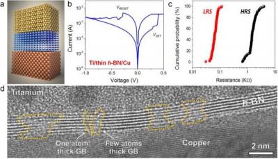
Researchers from Soochow University in China in collaboration with researchers form Harvard, Stanford and MIT developed RRAM memory devices using multilayer hexagonal boron nitride (h-BN) as dielectric. The devices show promising performance - while being based on a 2D material, which may pave the way towards extremely thin and efficient memory devices.

h-BN enables a 2D RRAM device image

2D materials (such as h-BN and others) are interesting to many researchers, and the field is experiencing a boom following the "discovery" of graphene in 2004.

Read the full story Posted: Mar 10,2017

Used egg shells used to create RRAM devices

Researchers from the Guizhou Institute of Technology in China produced RRAM devices using finely ground used egg shells. These devices were not very durable - they only lasted about 100 write cycles...

To create the devices, the researchers ground the egg shells until they got a 'nanoscale' powder. They then dried it and dissolved it in a solution. The solution was than used to coat a substrate to form the electrolyte part of the RRAM device.

Read the full story Posted: Jan 21,2017